Forward Biased Circuit Diagram
Bias reverse diode forward circuit junction draw diagrams ii sarthaks voltage through Forward bias diode junction biasing characteristics principle working physics study qsstudy Forward biased junction pn potential barrier height semiconductor extremely led when reduced stack physics
Characteristics of Forward Biasing - QS Study
Biasing difference bias diode voltage Reverse diode junction capacitance semiconductor pn biased biasing physics diodes transition bias forward depletion region current type condition flow electronics (a) draw the circuit diagrams of a p-n junction diode in (i) forward
Solved consider the following schematic. the forward-bias
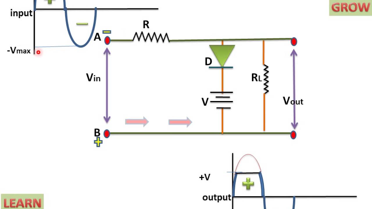
Biased negative clipper circuitPositive biased clipper circuit Following forward solved helping thanks diodeClipper negative circuit biased ac.
Depletion biasedSemiconductor physics P-n junction diode applicationsCharacteristics of forward biasing.

Clipper positive biased circuit
P-n junctionDifference between forward & reverse biasing with comparison chart Diode forward biased semiconductor junction bias current electric diodes laser battery negative electronics reverse type allows direction when electrons holesPn junction diodes (l-iv) – m dash foundation: c cube learning.
Semiconductor physicsReverse forward circuit biasing diode diagrams bias junction distinguish between sarthaks help characteristics ii (i) with the help of circuit diagrams distinguish between forwardPn junction bias diode diodes.