Forward Bias Circuit Diagram
Multisim bias diode zener Biasing difference bias diode voltage Multisim diode zener bias circuit
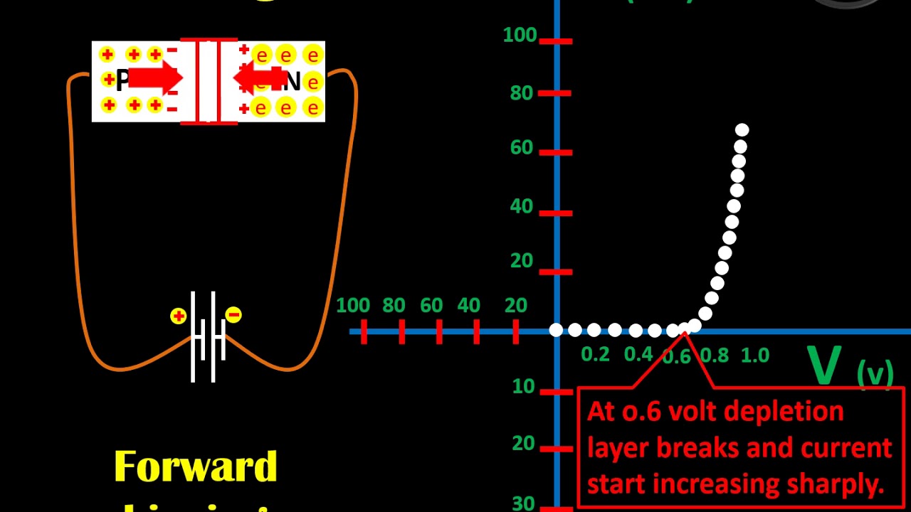
PN JUNCTION DIODE AND VI CHARACTERISTICS » PIJA Education
Diode forward bias circuit pn junction characteristics battery circuits Miirbe: pn junction diode forward bias circuit diagram To draw the i-v characteristic curve of a p-n junction in forward bias
Reverse forward circuit biasing diode diagrams bias junction distinguish between sarthaks help characteristics ii
Zener diode circuit forward biasRectifier diode : circuit diagram, biasing and its applications Bias diodeBias reverse forward pn junction diode condition electronics basic.
Circuit bias reverse diagram forward characteristics diode lab techZener diode forward bias circuit A bias circuit and b start-up circuit [19]What is the effect of forward and reverse biasing on depletion layer?.
![a Bias circuit and b start-up circuit [19] | Download Scientific Diagram](https://i2.wp.com/www.researchgate.net/profile/Mohammad_Hossein_Maghami/publication/257514349/figure/fig26/AS:667131595210768@1536067975966/a-Bias-circuit-and-b-start-up-circuit-19.png)
Pn bias junction characterist
Depletion biasing junction effectDifference between forward & reverse biasing with comparison chart Junction bias characteristic pn diode biasedTech lab: experiment 3: v-i characteristics of silicon semiconductor diode.
Pn junction diode and vi characteristics » pija education(i) with the help of circuit diagrams distinguish between forward Basic electronics.