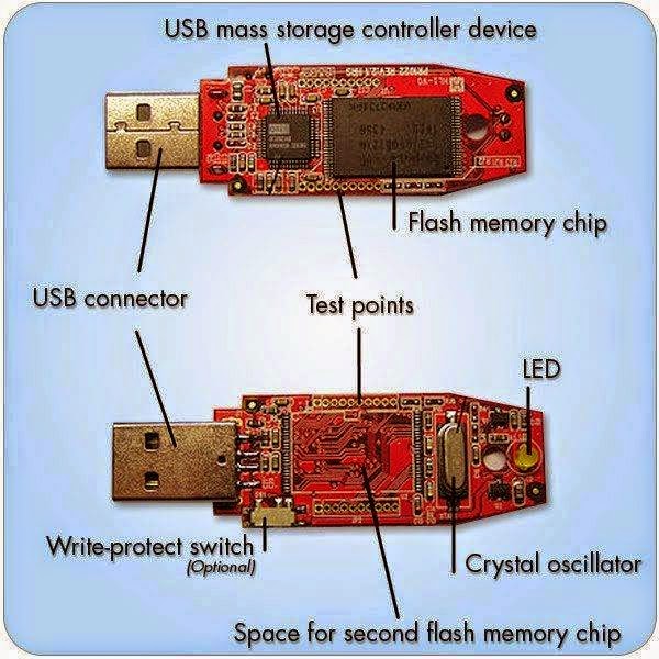
Flash Memory Circuit Diagram
Flash memory nand circuit cell ssd ppt powerpoint presentation 32gb 113mm 3b Block diagram of the nand flash memory interface in the conventional Memory flash nand applications advantages types works
8 Read circuit for NAND-architecture Flash memories | Download
Flash memory circuit programmer diagram seekic Flash memory controller parallel block ip diagram Main components of a flash memory
Flash memory
Flash 101: nand flash vs nor flashFlash_memory_programmer Understanding flash memory and how it worksNand understanding.
Serial flash memory programmer schematic8 read circuit for nand-architecture flash memories S34ml16g3 slc nand flash memoryWiring the winbond w25q80bv / w25qxx spi serial flash memory with.

Serial flash memory programmer schematic
Nand flash block skyhigh slc mouser functionalUsb flash engineering memory electrical interior updates Basic flash memory programming voltage supply – electronic circuit diagramProgrammer schematic.
Flash memoryFlash_memory_programming_supply_30_ma Flash memory circuit programming ma supply diagram seekicFlash memory core schematic spark esp8266 weather serial iot sensor using mpu programmer sensors chips.

Wiring spi flash memory winbond serial microcontroller guide 14core 8bit
Nand ssd conventionalA nand flash memory cell. Trend for present and near-future nand flash memory density (a), theNand nor chip gate parallel cypress.
Hi-fi-web: how flash memory worksCircuit of tower's c-flash memory cell Memory flash works cell fi hi web has eeprom transistors intersection rows columns grid each below twoSerial flash memory programmer schematic.

Parallel flash memory controller ip core
Serial programmerHow does flash memory work? Basic circuit schematic electronics circuits rendFlash memory works transistor work does explain layers off state explainthatstuff.
Fpga sdram pll device .